(Hong Kong)

Product Summary
The CXD5143GG-T2 is an audio decoder LSI that achieves super-low power consumption and supports many codecs. Useful interface such as NAND/NOR flash memory and Memory Stick is supported, and it comprises analog circuits such as audio D/A converter and SAR A/D converter. The CXD5143GG-T2 is suitable for portable audio players and cellular phone audio backend.
Parametrics
CXD5143GG-T2 absolute maximum ratings: (1)Digital I/O power supply 0 to 2, DVDIO0-2: -0.3 to 4.0 V; (2)Digital core power supply 0 to 2, DVDK0-2: -0.3 to 1.68 V; (3)Digital input voltage, SCL/GPIOK0, SDA/GPIOK1, DIV: -0.3 to 7.0 V; All other digital inputs: -0.3 to 4.0 V; (4)Digital output voltage, High output, DOV: DVDIO0-2 + 0.3 V; Low output: -0.3V; (5)Audio LPF power supply, AVDLPF: -0.3 to 3.6 V; (6)SAR A/D converter power supply, AVDADC: -0.3 to 1.68 V; (7)Main oscillator power supply, AVDOSC1: -0.3 1.68 V; (8)Sub oscillator power supply, AVDOSC2: -0.3 1.68 V; (9)PLL power supply, AVDPLL: -0.3 to 1.68 V; (10)USB PHY power supply, AVDUSB: -0.3 to 3.6 V; (11)Storage temperature, Tstg: -40 +150℃.
Features
CXD5143GG-T2 features: (1)CPU: ARM7TDMI; (2)RAM: 320K bytes; (3)ROM: 448K bytes; (4)Frequency: 45.1584MHz; (5)Peripherals, Host interface: SRAM, NOR flash slave compatible Host processor can be connected; (6)General-purpose I/O: 116 (When all multiplexed pins are set as GPIO), Direction individually selected; (7)Signal processing accelerator: Virtual Mobile Engine; (8)Oscillator, Main: 45.1584MHz input, Crystal/Ceramic selectable; Sub: 12MHz input, Crystal/Ceramic selectable; (9)Process: CMOS 0.13μm.
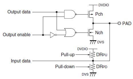
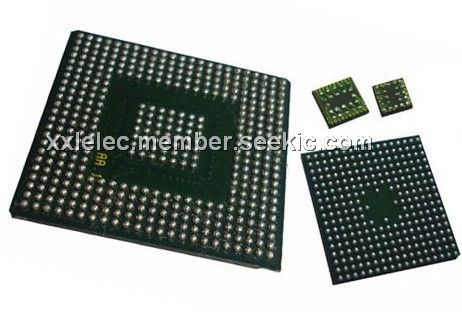
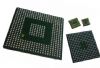
Diagrams