(Hong Kong)

Product Summary
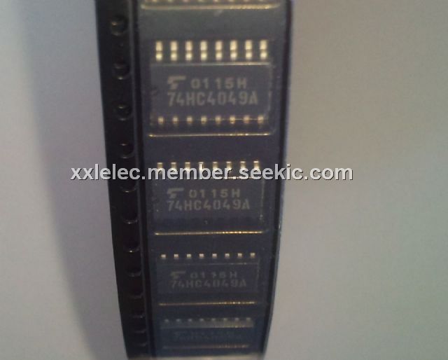
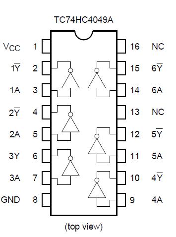
The 74HC4049A is a high speed CMOS HEX BUFFER fabricated with silicon gate C2MOS technology. The 74HC4049A achieves the high speed operation similar to equivalent LSTTL while maintaining the CMOS low power dissipation. The device is an inverting buffer The internal circuits are composed of 3-stages of invertaers, which provided high noise immunity and stable output. Input protection circuits are different from those of other high speed CMOS IC’s. The 74HC4049A eliminates the diodes on the VCC side thus providing of logic-level conversion from high-level volages up to 15 V to low-level voltages.
Parametrics
74HC4049A absolute maximum ratings: (1)Supply voltage range, VCC: -0.5 to 7 V; (2)DC input voltage, VIN: -0.5 to 18 V; (3)DC output voltage, VOUT: -0.5 to VCC + 0.5 V; (4)Input diode current, IIK: -20 mA; (5)Output diode current, IOK: ±20 mA; (6)DC output current, IOUT: ±35 mA; (7)DC VCC/ground current, ICC: ±75 mA; (8)Power dissipation, PD: 500 (DIP) (Note 3)/180 (SOP/TSSOP) mW; (9)Storage temperature, Tstg: -65 to 150℃.
Features
74HC4049A features: (1)High speed: tpd = 9 ns (typ.) at VCC = 5 V; (2)Low power dissipation: ICC = 1μA (max) at Ta = 25℃; (3)High noise immunity: VNIH = VNIL = 28% VCC (min); (4)Output Drive Capability: 15 LSTTL loads; (5)Symmetrical output impedance: |IOH| = IOL = 6 mA (min); (6)Balanced propagation delays: tpLH to tpHL; (7)Wide operating voltage range: VCC (opr) = 2 V to 6 V; (8)Pin and function compatible with 4049B/4050B.
Diagrams
 |
 74HC |
Other |
|
Data Sheet |
Negotiable |
|
||||
|
74HC/HCT02 |
Other |
|
Data Sheet |
Negotiable |
|
||||
|
74HC/HCT03 |
Other |
|
Data Sheet |
Negotiable |
|
||||
|
74HC/HCT10 |
Other |
|
Data Sheet |
Negotiable |
|
||||
|
74HC/HCT107 |
Other |
|
Data Sheet |
Negotiable |
|
||||
|
74HC/HCT109 |
Other |
|
Data Sheet |
Negotiable |
|
||||